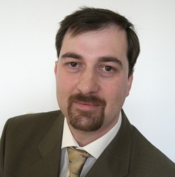
Michael Kogan
Key points:
- Expert for Physical Implementation(place and route), and Design for Test(DFT) of digital ICs
- More than 12 years experience
- More than 20 projects
- More than 30 satisfied customers in Europe, Russia and Midle East.
Fields of Expertise:
- Physical Implementation of Digital IC
- Synthesis, STA, placement, power and detail route, timing closure, signal integrity,
physical verification, timing and power analysis, test insertion, test vectors generation and simulation.
- Design for both high-performance and ultra-low-power devices.
- Complex multi-million gates SOC and low power designs at 180nm - 65nm technologies
- Flat and hierarchical designs implementation.
- Design for Test (DFT) expert:
- Setup test concept for complex designs
- Scan-chains insertion with and without compression logic
- Boundary Scan insertion and test vectors generation
- Power domain aware scan-chain insertion and test vectors generation
- Automatic Test Pattern Generation (ATPG) for stuck-at, at-speed, Iddq
- Flow and Methodology setup.
- Technical and Project Lead for local and international team.
- Expert of Cadence digital IC implementation tools: RTL Compiler, SOC Encounter,
Conformal, Encounter Test etc.
Major Projects:
- Physical implementation (RTL to GDSII) or multimilion instance chips for Telecomunication
and Network Processing designs at TSMC 90nm-65nm technology
- Low power design
- Delay(at-speed) and stuck-at ATPG for very complex design.
- Customer ramp-up on Cadence refernce flow and tools.
| 
|

